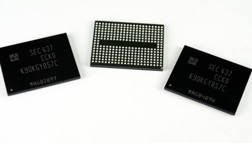
Best of both worlds: Samsung announces production of three-bit, 3D, high-density NAND flash
One note is that Samsung is attempting to have its cake and eat it too as far as the NAND is concerned, referring to this as “3-bit multi-level cell (MLC).” That’s not how the term is typically used, and until Samsung demonstrates that it’s built TLC NAND with MLC characteristics in both performance and longevity, it’s a misapplication of terminology for the sake of marketing.
Underneath that marketing, however, there is reason to think that TLC built vertically could be superior to its traditional planar counterpart. Samsung’s 850 Pro, the first SSD to use V-NAND, has substantially better reliability and performance than traditional planar counterparts. If Samsung can keep those characteristics and extend them into a TLC drive, it could create the most attractive consumer drive on the market.
Samsung’s PR also inadvertently highlights the misleading ways that process nodes are used to market to consumers. While it claims that its 3D NAND is more than twice as productive per wafer as its 10nm-class NAND, an editor’s note remarks that “10 nanometer-class means a process technology node somewhere between 10 and 20 nanometers.” Independent analysis from Anandtech has shown that Samsung’s V-NAND has a very small die advantage over the leading 16nm NAND from Micron.

